 Academia
 Ai
Ai
 Astronomy
 Biology
 Chemistry
 Climate
 Conspiracy
 Earth-science
 Engineering
 Evolution
 Geology
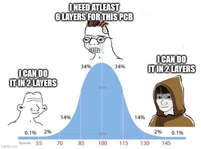
The eternal struggle between engineers and PCB designers in one beautiful bell curve. In the middle, we have the reasonable engineer desperately pleading for 6 layers to make a functional printed circuit board. Meanwhile, at both extremes of the IQ distribution, we find the geniuses (or idiots?) confidently claiming they can do it in just 2 layers.
This is electrical engineering's version of the Dunning-Kruger effect – where the truly incompetent and the legitimate savants arrive at the same conclusion through wildly different paths. One will create a rat's nest of copper traces that violates every design rule in existence; the other will produce an elegant masterpiece of minimalist engineering that somehow works flawlessly.
The true pain comes when the project manager sides with the 2-layer crowd because "it's cheaper" and then wonders why the board keeps failing EMC testing...